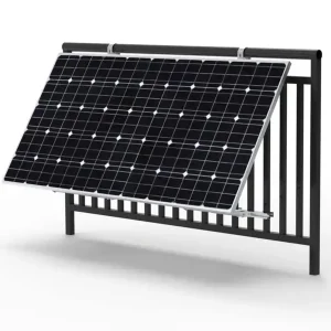
In the contemporary landscape of renewable energy, the efficiency of solar modules is no longer just about the absorption capability of silicon wafers; it is fundamentally governed by the intelligent management of shading and thermal protection. As a leading OEM/ODM Bypass Diode Panel Technology Manufacturer, Jiangsu Vires Energy Co., Ltd. is at the forefront of this technical evolution. Bypass diodes are critical components integrated into solar junction boxes to prevent the "hot-spot effect," which occurs when a cell is shaded and begins to consume power instead of generating it, leading to potential structural damage and fire hazards.
The global industrial status of bypass diode technology has transitioned from simple Schottky Barrier Diodes (SBD) to sophisticated Active Bypass Integrated Circuits (ICs). This transition is driven by the need for higher current handling capacities in ultra-high-power modules (600W+) and the stringent reliability requirements of utility-scale solar farms.
Advanced heat dissipation techniques in junction boxes ensure that diodes remain below critical temperatures during bypass events, extending the panel's lifespan to 25+ years.
Utilizing low-VF Schottky diodes reduces power loss during shading, directly improving the Levelized Cost of Energy (LCOE) for commercial solar projects.
Tailored diode configurations for half-cut cells, shingled modules, and bifacial technologies to optimize the specific electrical characteristics of each panel design.
The industry is moving toward "Smart Modules" where bypass diodes are replaced by DC Optimizers or Smart Bypass ICs. These devices provide module-level monitoring and rapid shutdown capabilities, meeting the latest NEC safety standards in the USA and European IEC regulations.
Reliability Rate in Extreme Climates
Typical Forward Voltage Drop
Jiangsu Vires Energy Co., Ltd. is a leading manufacturer specializing in home solar power systems with nearly 20 years of experience in the renewable energy industry. We are recognized as one of the top manufacturers in China and have established branch offices and after-sales service centers in key global markets, including Pakistan, South Africa, Germany, the Netherlands, and the USA.
Sorting
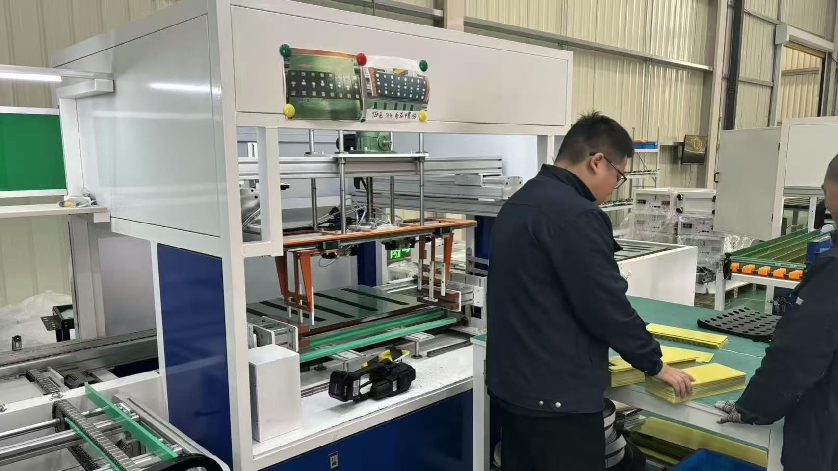
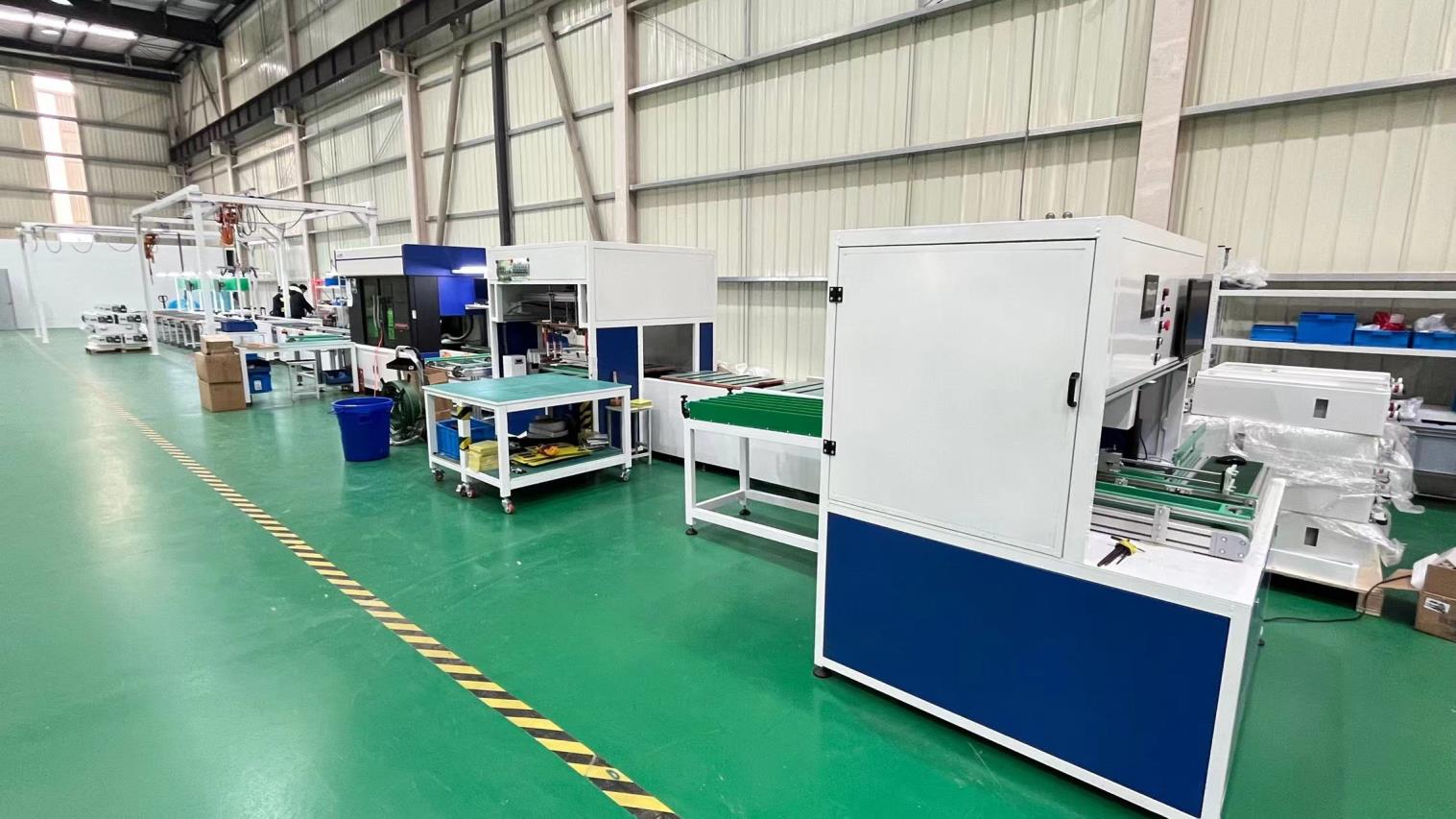
Extrusion Process
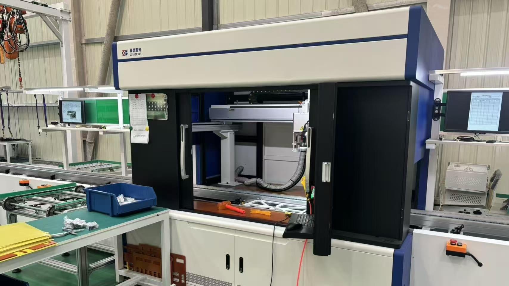
Laser Welding
Assemble
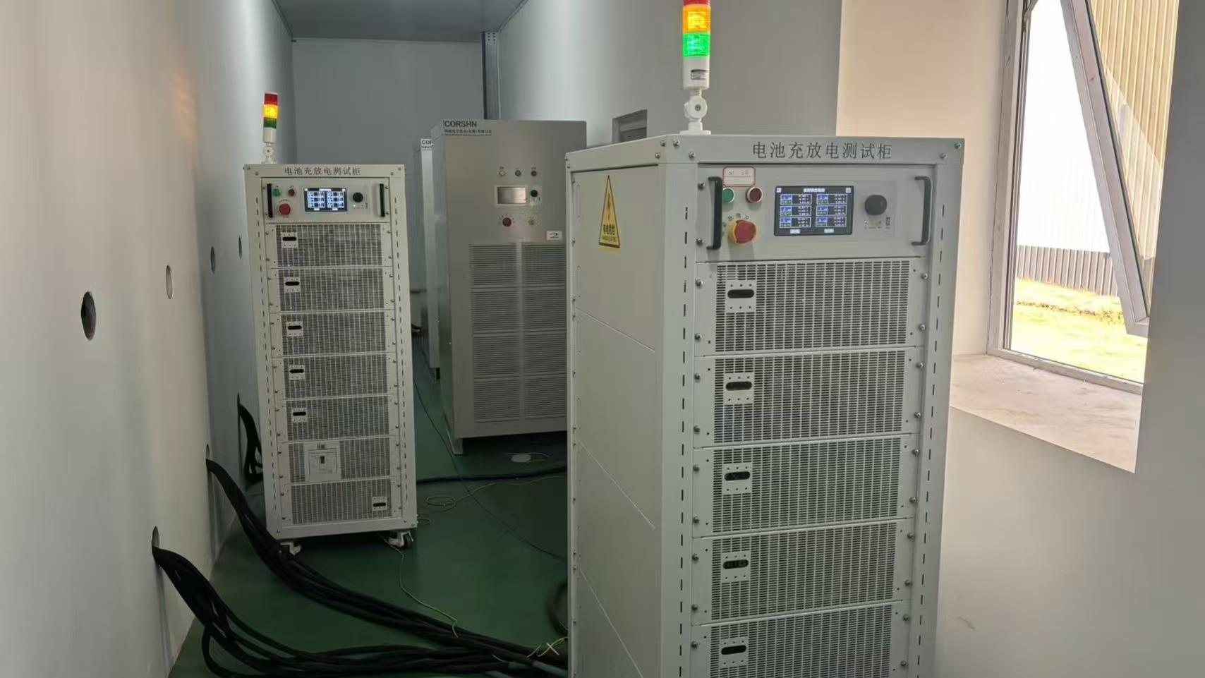
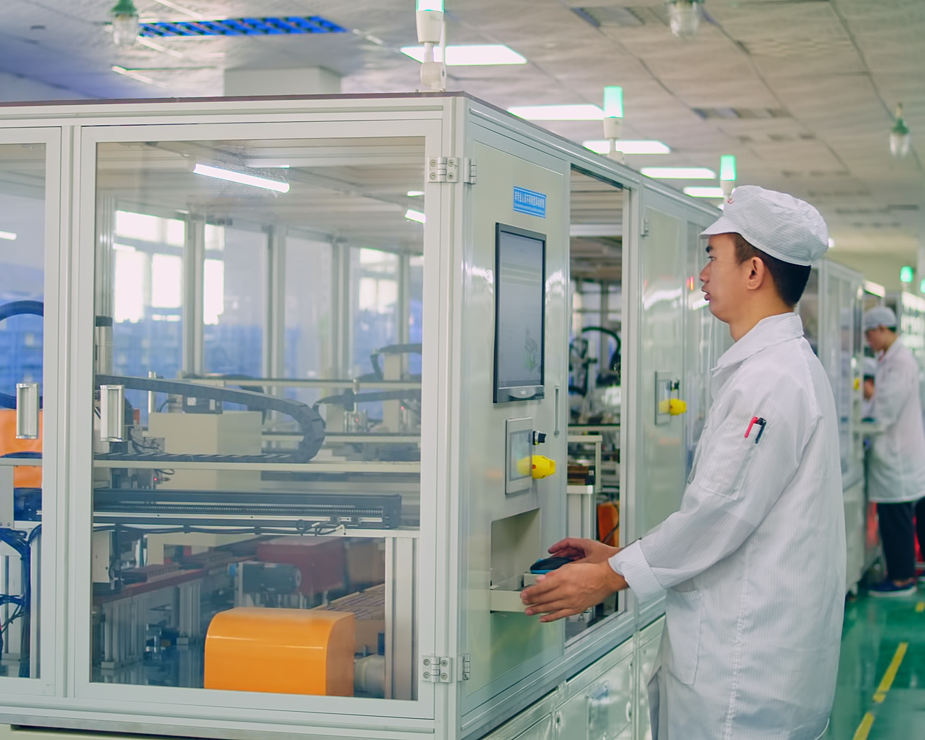
Aging Test
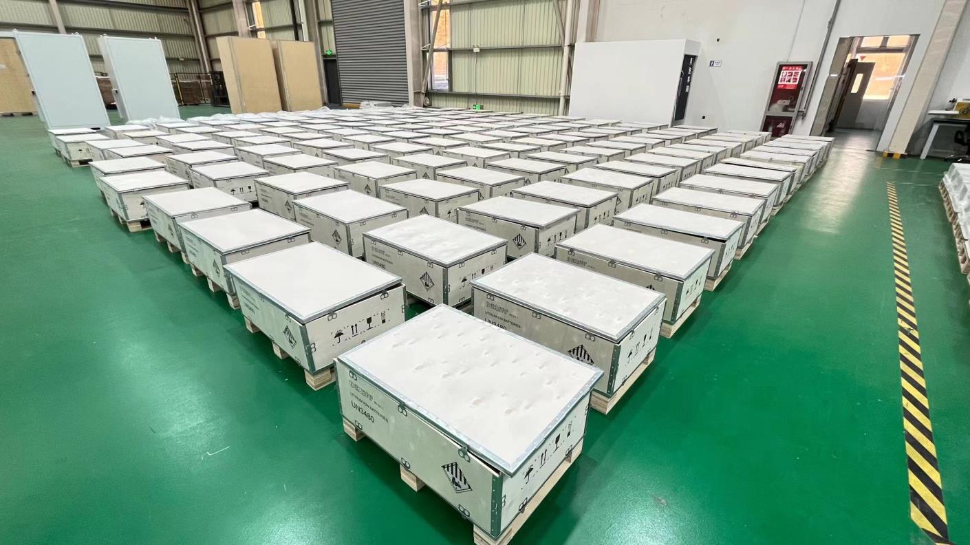
Packaging
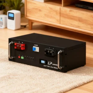
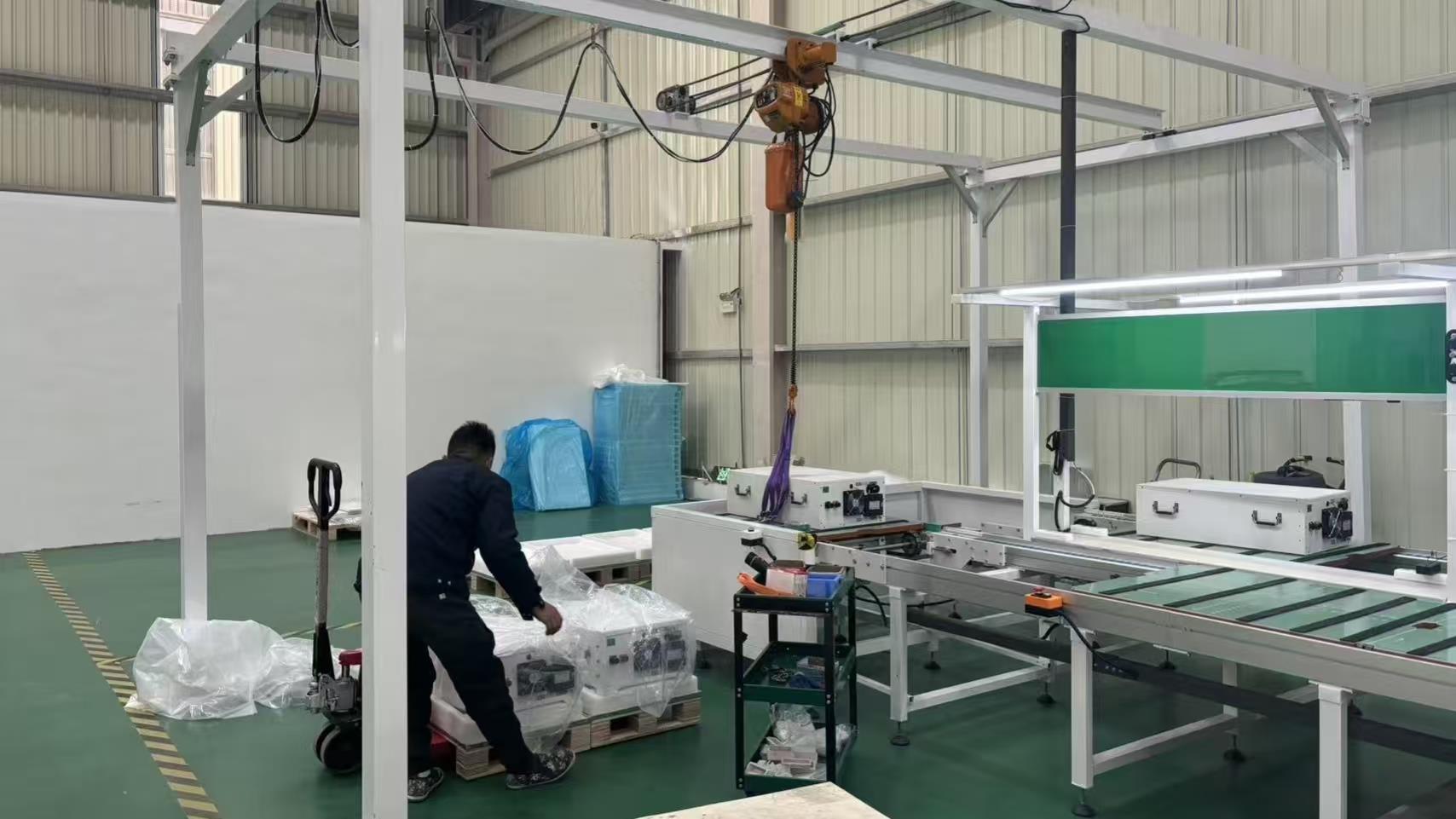
Battery production line
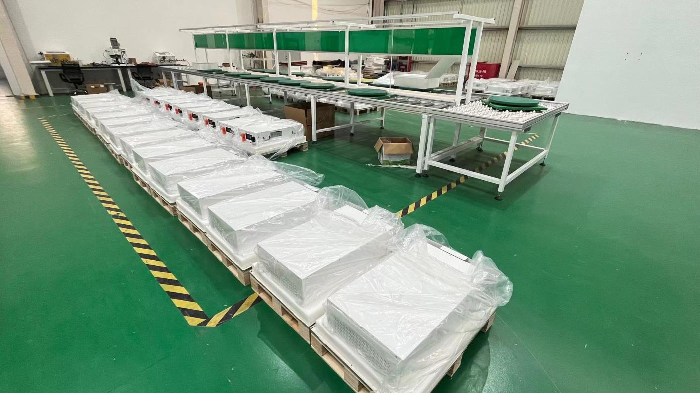
High-voltage box production
As the solar industry moves towards TOPCon and HJT (Heterojunction Technology), the role of the bypass diode has become more complex. High-efficiency cells have different reverse bias characteristics, requiring manufacturers to recalibrate diode response times to prevent micro-cracks during shading.
Our OEM/ODM solutions provide Custom Junction Box Integration. We don't just supply a diode; we provide a thermal management ecosystem. For utility-scale projects in MENA regions, where ambient temperatures exceed 50°C, our bypass diode technology incorporates advanced potting compounds that enhance thermal conductivity, ensuring the diodes don't reach their "thermal runaway" point.
In floating solar applications, our IP68-rated waterproof junction boxes with integrated bypass protection prevent moisture ingress while maintaining high electrical efficiency. This holistic approach to Search Intent Mining reveals that engineers aren't just looking for "diodes," they are looking for "long-term system reliability."
A: Most modules are divided into three series-connected cell strings. One diode is placed in parallel with each string. If one string is shaded, its diode conducts, allowing the current from the other two strings to "bypass" the shaded one, preventing power loss for the entire module.
A: Schottky diodes have a much lower forward voltage drop (approx. 0.4V vs 0.7V for Silicon). In a solar panel, this lower voltage drop means less power is wasted as heat during bypass mode, leading to higher efficiency and safer operating temperatures.
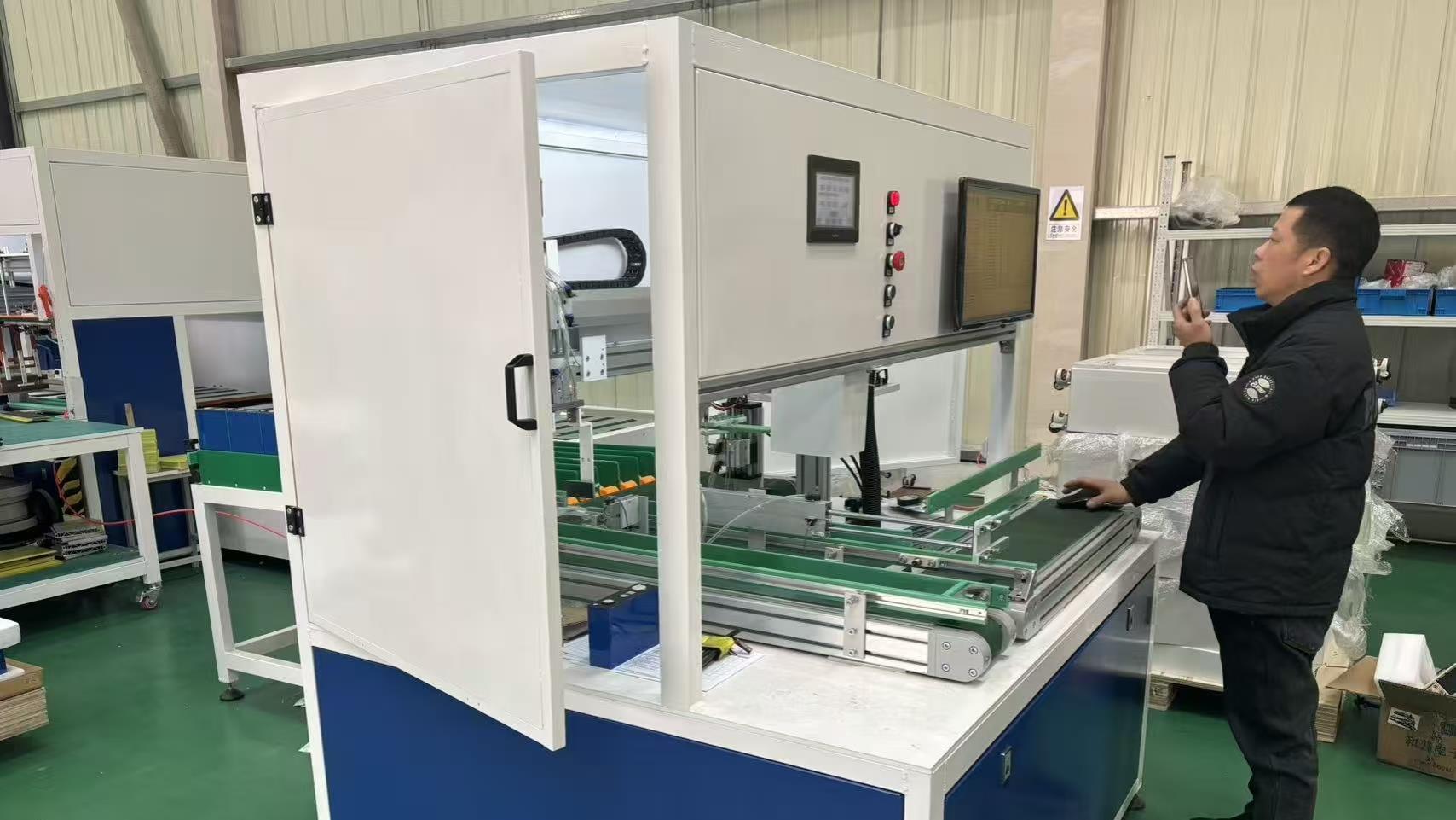
A: We utilize 100% Electroluminescence (EL) testing and Thermal Imaging during the bypass test phase. This ensures no localized hot spots exist before the panel leaves our facility.